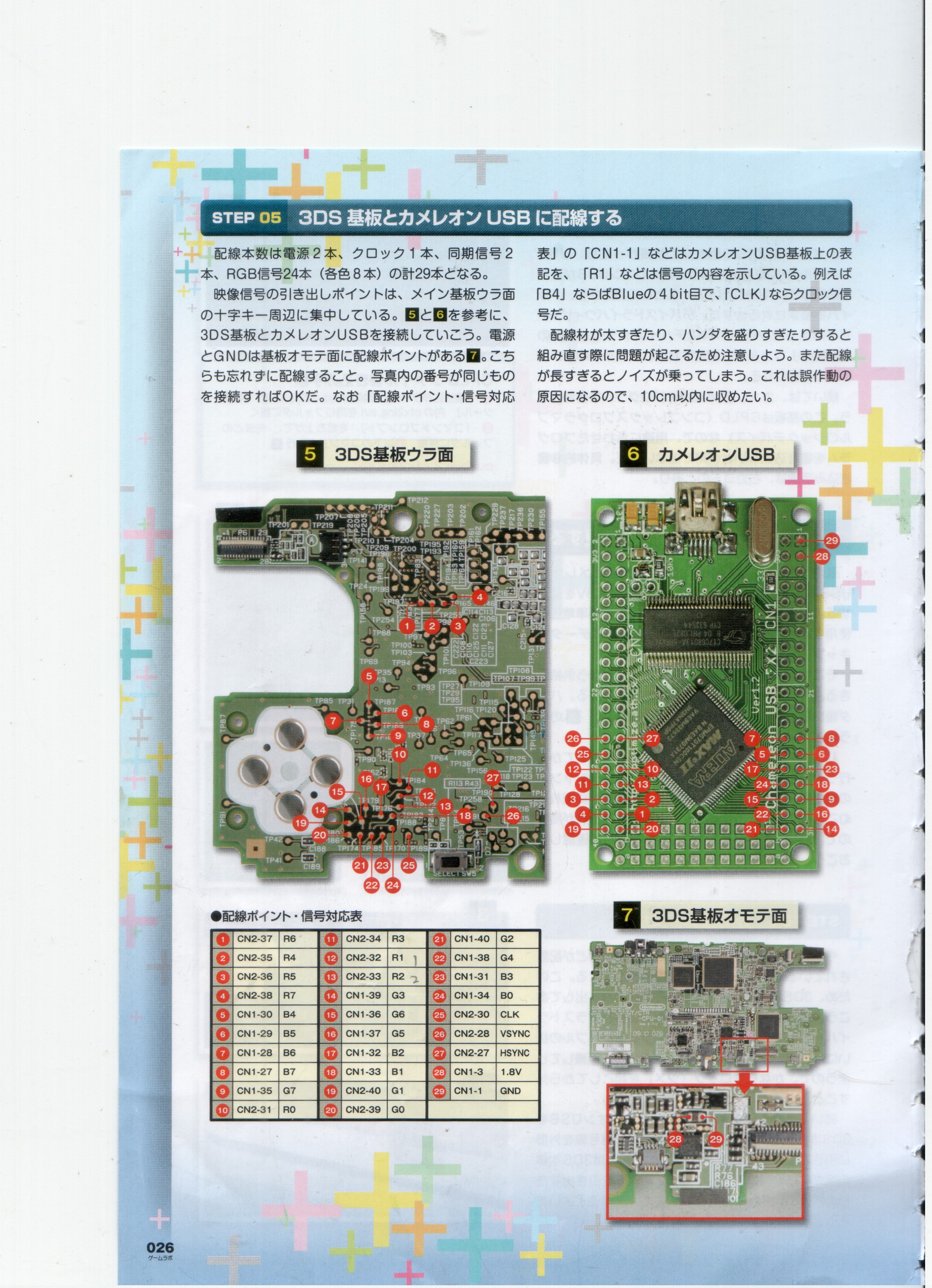
This page documents the procedure of capturing the video signal of the upper and lower screens of the 3DS.
The information on this page was found by 3DBrew User: Matyapiro31

Lower Screen Dump #
Test Points on the front of the board:
| # | Name | TP | RED | # | Name | TP | GREEN | # | Name | TP | BLUE |
|---|---|---|---|---|---|---|---|---|---|---|---|
| 10 | CN2-31 | 184 | R0 | 20 | CN2-39 | 186 | G0 | 24 | CN1-34 | 188 | B0 |
| 12 | CN2-32 | 178 | R1 | 19 | CN2-40 | 180 | G1 | 18 | CN1-33 | 182 | B1 |
| 13 | CN2-33 | 172 | R2 | 21 | CN1-40 | 174 | G2 | 17 | CN1-32 | 176 | B2 |
| 11 | CN2-34 | 166 | R3 | 14 | CN1-39 | 168 (above 180) | G3 | 23 | CN1-31 | 170 | B3 |
| 2 | CN2-35 | 183 | R4 | 22 | CN1-38 | 185 | G4 | 5 | CN1-30 | 187 | B4 |
| 3 | CN2-36 | 177 | R5 | 16 | CN1-37 | 179 | G5 | 6 | CN1-29 | 181 | B5 |
| 1 | CN2-37 | 171 | R6 | 15 | CN1-36 | 173 (below 179) | G6 | 7 | CN1-28 | 175 | B6 |
| 4 | CN2-38 | 165 | R7 | 9 | CN1-35 | 167 | G7 | 8 | CN1-27 | 169 | B7 |
| # | Name | TP | Description |
|---|---|---|---|
| 25 | CN2-30 | 189 | CLK |
| 26 | CN2-28 | 191 | VSYNC |
| 27 | CN2-27 | 190 | HSYNC |
This table (taken from the picture above) shows which TP (test-point) to get the bit of the corresponding color (R=red, G=green, B=blue).
And the TP to get Clock, Vertical-Sync and Horizontal-Sync.
Captured Video Control Signals #
The following picutres show plots of the control signals CLK (TP189), HSYNC (TP190) and VSYNC (TP191). The used sample rate were 50MHz.
The full plot shows about 2.6ms.

This plot shows 1.28us, mainly featuring the clock

Setup
The signal capturing was done by using an DE10-NANO FPGA development board, Intel signal tap analyzer and 5 wires soldered to the TPs of an EU-O3DS (roughly 25cm long, parallel wired).
VCD and CVS files: Media: Stp_PCLK_VSYNC_HSYNC.7z (to view the VCD file use GTK Wave or similar programs).
Links #
- DS Version (DSCapture): 🔗 http://www.3dscapture.com/ds
- DS Version(NisetroCaptureDS): 🔗 http://www.3dsvideocapture.com/product-list/1
- DSi Version(NisetroCaptureDSi): 🔗 http://www.3dsvideocapture.com/product-list/2
- 3DS Version(NisetroCapture3DS): 🔗 http://www.3dsvideocapture.com/product-list/3
- New3DS Version(NisetroCaptureNew3DS): 🔗 http://www.3dsvideocapture.com/product-list/12
- New3DS XL Version(NisetroCapturenew3DSXL): 🔗 http://www.3dsvideocapture.com/product-list/11
- Pics+Progress Updates (3DSCapture): 🔗 http://www.3dscapture.com/
- YouTube video of Loopy’s Device (USB): 🔗 http://www.youtube.com/watch?v=mT0DuQleuhY
- YouTube video of Loopy’s Device (HDMI): 🔗 http://www.youtube.com/watch?v=s99fUS68AB4